When converting computer switching power supplies (hereinafter referred to as UPS) with a TL494 control chip into power supplies for powering transceivers, radio equipment and chargers for car batteries [1], a number of UPSs accumulated that were faulty and could not be repaired, were unstable or had a control a different type of chip.
They also got around to the remaining power supplies, and after some experimentation they developed the technology for converting them into chargers (hereinafter referred to as chargers) for car batteries. Also, after the publication of my article “PC UPS for amateur radio purposes on TL494 with voltage and current stabilization,” letters began to arrive by email with various questions, like what and how, where to start.
↑ Let's understand the impulse circuit
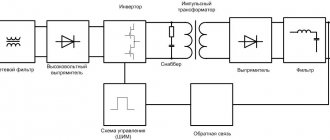
The UPS circuit can be divided into the following main parts: - input noise suppression filter (not always installed by the manufacturer); — network rectifier; — smoothing capacitive filter; — key voltage converter with a pulse power transformer (power inverter); — matching cascade; — control circuit; — circuits for generating output voltages and transmitting a feedback signal to the control circuit; — output rectifier with filter; — auxiliary converter (not available in AT type power supply units).
The input circuits (Fig. 1) include: an input noise suppression filter (circled by a dotted line in the diagram), a network rectifier, a smoothing capacitive filter.
The thermistor TR1 with a negative TCS serves to limit the surge of charging current through capacitors C5 and C6. In a cold state, the resistance of the thermistor is several Ohms; the charging current through the rectifying diodes of the VDS1 bridge is limited to a level that is safe for them. As a result of current flowing through the thermistor, it heats up and its resistance decreases to fractions of an Ohm and subsequently has virtually no effect on the operation of the UPS circuit. The mains fuse FU1 is designed to protect the supply network from overload in the event of possible short circuits in the primary circuit of the UPS, but does not actually prevent the rectifier diodes and key transistors from breaking down when the output is overloaded.
↑ Input noise filter
prevents the penetration of high-frequency impulse noise from the network into the UPS and from the UPS into the network, but in practice it is very often found that manufacturers (aka the Chinese) do not install a filter in order to save money, although there is a place for it, and the windings Dr1 are replaced with jumpers, thereby worsening EMC around. Thanks to Chinese savings on power filter parts, now the noise level in the city on the 160 and 80 m bands reaches 57 - 59 on the receiver's S-meter scale, this excludes the possibility of normal reception in urban conditions on these bands.
↑ Key voltage converter
with a pulse power transformer (power inverter) is built using a push-pull half-bridge circuit, the main difference lies in the circuit design solutions for constructing the basic circuits of power key transistors.
The configuration of the base circuits is determined by the type of UPS starting circuit. Fragment excluded. The full version of the article is available to patrons and full members of the community. Read the terms of access.
↑ Output rectifier with filter
built approximately according to the same scheme (Fig. 4) with minor variations. The rectifiers are built according to a full-wave circuit with a midpoint, this ensures a symmetrical mode of magnetization reversal of the core of the pulse power transformer Tr. To reduce dynamic switching losses in the high-current channels of the + 12 and + 5 V rectifiers, diode assemblies of two Schottky diodes VD3 and VD4 are used as rectifier elements, since they have a very short switching time, and the forward voltage drop across the Schottky diode is 0.3 - 0.4 V, which, in contrast to a conventional silicon diode (the forward voltage drop across which is 0.8 - 1.2 V) with a load current of 10 - 20 A, gives a gain in UPS efficiency. All rectified voltages are smoothed by LC filters, which starts with inductance. The inductor windings for rectifiers + 5, - 5, + 12 and - 12 V are usually wound on one magnetic core.
The UPS produces the main voltages +5 V, -5 V, +12 V, -12 V, in new ATX units there is also + 3.3 V, the Power good (PG) signal, etc. We are primarily interested in the +12 voltage generation channel B, we will mainly work with him. The output voltages of the UPS are supplied to the nodes and computer unit using multi-colored wires assembled into bundles.
↑ Six-pin connectors
(absent in UPS series ATX) have the following color markings: +5 V - red; +12 V - yellow; -5 V - white; -12 V - blue; PG - orange; GND (body, ground) - black; Four-pin connectors are color coded as follows: +5 V - red; +12 V - yellow; GND (body, ground) - black;
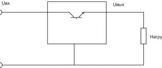
How to turn on the power supply from a computer without a computer
So, we have in our hands an ATX computer power supply. First of all, let's try to turn it on. But to do this you need to know some of the intricacies of how this device works. Suppose we have a computer in front of us. We plug it into the network, but outwardly nothing happens. This would seem to be clear - the machine is turned off, and to turn it on, you need to press the power button on the front panel of the system unit.
Actually this is not true. As soon as we inserted the plug into the socket, a small part of the circuit in the power supply started working, producing a standby voltage of +5 V. This part is called the standby power module. Voltage is supplied to the motherboard and powers its individual components, one of which is designed to turn on the computer.
Important. Most ATX power supplies have an additional service mechanical switch located on the back of the PC. The mains voltage is supplied to the power supply of these models after turning on this toggle switch.
A mechanical switch is used to supply voltage to this power supply.
By pressing the button on the front panel of the system unit, we thereby send a command to the motherboard (more precisely, its switching unit) to start the power supply. The node sends a Power on signal to the power supply unit, and the power supply unit, and therefore the computer itself, turns on.
Since we don’t have a computer, we will have to send this signal ourselves. This is not difficult to do. To do this, just find the connector on the power supply that powers the motherboard and install a jumper between the green and any of the black wires. So, we install a jumper, connect the power supply to the network, and it starts up immediately - you can hear it even from the noise of the fan.
↑ Our memory scheme
Fragment excluded. The full version of the article is available to patrons and full members of the community. Read the terms of access.
And so let’s consider the case when the battery is not yet connected. The AC mains voltage is supplied through the thermistor TR1, mains fuse FU1, and noise suppression filter to the rectifier on the diode assembly VDS1. The rectified voltage is smoothed by a filter on capacitors C6, C7, and the output of the rectifier produces a voltage of + 310 V. This voltage is supplied to a voltage converter using powerful key transistors VT3, VT4 with a pulse power transformer Tr2.
Let’s immediately make a reservation that for our charger there are no resistors R26, R27, intended for slightly opening transistors VT3, VT4. The base-emitter junctions of transistors VT3, VT4 are shunted by circuits R21R22 and R24R25, respectively, as a result of which the transistors are closed, the converter does not work, and there is no output voltage.
When the battery is connected to the output terminals Cl1 and Cl2, the VD12 LED lights up, voltage is supplied through the VD6R16 chain to pin No. 12 to power the MC1 microcircuit and through the VD5R12 chain to the middle winding of the matching transformer Tr1 of the driver on transistors VT1, VT2. Control pulses from pins 8 and 11 of the MC1 chip are sent to the driver VT1, VT2, and through the matching transformer Tr1 to the base circuits of the power key transistors VT3, VT4, opening them one by one.
The alternating voltage from the secondary winding of the power transformer Tr2 of the + 12 V voltage generation channel is supplied to a full-wave rectifier based on an assembly of two VD11 Schottky diodes. The rectified voltage is smoothed out by the LC filter L1C16 and goes to the output terminals Cl1 and Cl2. The output of the rectifier also powers the standard fan M1, intended for cooling UPS parts, connected through a damping resistor R33 to reduce the rotation speed of the blades and fan noise.
The battery is connected through terminal Cl2 to the negative output of the UPS rectifier through resistor R17. When the charging current flows from the rectifier to the battery, a voltage drop is formed across resistor R17, which is supplied to pin No. 16 of one of the comparators of the MC1 microcircuit. When the charging current exceeds the set level (by moving the charge current setting resistor R4), the MC1 microcircuit increases the pause between output pulses, reducing the current to the load and thereby stabilizing the battery charging current.
Circuit R14R15 output voltage stabilization R14R15 is connected to pin No. 1 of the second comparator of the MC1 chip, designed to limit its value (at + 14.2 - + 16 V) in the event of the battery being disconnected. When the output voltage increases above the set level, the MC1 microcircuit will increase the pause between output pulses, thereby stabilizing the output voltage. Microammeter PA1, using switch SA1, is connected to different points of the UPS rectifier, and is used to measure the charging current and voltage on the battery.
As a PWM control regulator MC1, a microcircuit of the TL494 type or its analogues is used: IR3M02 (SHARP, Japan), µA494 (FAIRCHILD, USA), KA7500 (SAMSUNG, Korea), MV3759 (FUJITSU, Japan, KR1114EU4 (Russia).
Regulated power supply from ATX power supply on TL494. Part 1 - iron
Hi all! Today I would like to tell you about my experience of converting the most ordinary Chinese ATX power supply into an regulated power supply with current and voltage regulation (0-20A, 0-24V).
In this article, we will take a detailed look at the operation of the TL494 PWM controller, feedback and go over the modernization of the power supply circuit and the development of a home-made voltage and current error amplifier board.
To be honest, now I can’t even name the model of the experimental BP. One of the many cheap 300W P4 ready. I hope there is no need to remind you that in reality these 300W mean no more than 150, and then only with the appearance of a fried smell in the apartment.
I hope that my experience can be useful to someone from a practical point of view, and therefore I will focus on theory. Without it, you still won’t be able to remake the power supply because... in any case, there will be some differences in the circuit and difficulties during setup.
ATX power supply circuit
First, let's go through the ATX power supply circuit on the TL494 controller (and its numerous clones). All schemes are very similar to each other. Google brings up quite a lot of them and it seems I found one that almost matches my copy.
We will structurally divide the power supply into the following blocks: - mains voltage rectifier with filter - standby power supply (+5V standby) - main power supply (+12V, -12V, +3.3V, +5V, -5V) - main voltage control circuit, generation PowerGood signal and short circuit protection
The rectifier with filters is everything in the upper left corner of the circuit up to diodes D1-D4.
The standby power supply is assembled on transformer T3 and transistors Q3 Q4. Stabilization is based on feedback through the optocoupler U1 and the reference voltage source TL431. I will not consider the work of this part in detail because... I know that reading articles that are too long is not very fun. At the end I will give the title of the book where all the details are discussed in detail.
Please note that in the diagram, by mistake, both the PWM controller TL494 and the standby power supply ION TL431 are designated as IC1. In the future, I will mention IC1 referring specifically to the PWM controller.
The main power supply is assembled on transformer T1, high-voltage switches Q1 Q2, control transformer T2 and low-voltage switches Q6 Q7. This whole thing is swung and controlled by the PWM controller chip IC1. Understanding the principle of operation of the controller and the purpose of each element of its wiring is exactly what is necessary for conscious modification of the power supply instead of blindly repeating other people's recommendations and diagrams.
The mechanism of operation is approximately as follows: the PWM controller, alternately opening low-voltage switches Q6 Q7, creates an EMF in the primary winding of transformer T2. Do you see how these keys are powered by low voltage from the standby power supply? Find R46 on the diagram and you will understand what I mean. The PWM controller is also powered from this standby voltage. A little higher I called transformer T2 control, but it seems that it has some more correct name. Its main task is galvanic isolation of the low-voltage and high-voltage parts of the circuit. The secondary windings of this transformer control high-voltage switches Q1 Q2, opening them in turn. With this trick, a low-voltage PWM controller can control high-voltage switches in a safe manner. High-voltage switches Q1 Q2, in turn, swing the primary winding of transformer T1 and the main voltages that interest us arise on its secondary windings. These switches are called high-voltage because they switch rectified mains voltage, which is about 300V! The voltage from the secondary windings of T1 is rectified and filtered using LC filters.
Now, I hope you understand the overall picture and we can move on.
PWM controller TL494.
Let's figure out how the TL494 PWM controller works. It will be better if you download the datasheet www.ti.com/lit/ds/symlink/tl494.pdf, but in principle I will try to get the most important things out of it with the help of pictures. For a deeper understanding of all the subtleties, I recommend this document: www.ti.com/lit/an/slva001e/slva001e.pdf
Let's start, oddly enough, from the end - with the output part of the microcircuit. Now all attention is paid to the output of the OR element (marked with a red square). The output of this element at a specific point in time directly controls the state of one or both keys Q1 Q2. The control option is set via pin 13 (Output control).
Important thing No. 1: if the output of the OR element is log 1, the output keys are closed (turned off). This is true for both modes. Important thing No. 2: if the output of the OR element is log 0, one of the keys (or both at once) is open (enabled).
The following picture emerges: along the rising edge, the previously open transistor closes (at this moment they are both guaranteed to be closed), the trigger changes its state and, along the descending edge, another switch is turned on and will remain on until the rising edge comes again and closes it, at which time moment again the trigger clicks and the next descending edge will open another transistor. In single ended mode, the keys always work synchronously and the trigger is not used.
The time when the output is in the log. 1 (and both keys are closed) is called Dead time. The ratio of the pulse duration (log 0, transistor open) to the period of their repetition is called the duty cycle (PWM duty cycle). For example, if the coefficient is 100%, then the output of the OR element is always 0 and the transistor (or both) is always open.
Sorry, but I try to explain it as clearly as possible and almost on the fingers, because in official dry language it can be read in the datasheet.
Oh yes, why do we need Dead time? In short: in real life, the top key will pull up (toward the plus) and the bottom key down (to the minus). If you open them at the same time, there will be a short circuit. This is called through current and due to parasitic capacitances, inductances and other features, this mode occurs even if you open the keys strictly one by one. To minimize through current, dead time is needed.
Now let's turn our attention to the saw generator (oscillator), which uses pins 5 and 6 of the microcircuit to set the frequency. A resistor and capacitor are connected to these terminals. This is the same RC generator that many have probably heard about. Now at pin 5(CT) we have a saw from 0 to 3.3V. As you can see, this saw is fed to the inverting inputs of the Dead-time and PWM comparators.
We have more or less decided on the terms and operation of the output part of the PWM controller, now we will figure out what the saw has to do with it and why we need all these comparators and error amplifiers. We realized that the ratio of the pulse duration to the period of their repetition determines the duty cycle, and therefore the output voltage of the power source because The higher the fill factor, the more energy will be pumped into the primary winding of the transformer.
For example, let's figure out what needs to be done to set the fill factor to 50%. Do you still remember about the saw? It is supplied to the inverting inputs of the PWM and Dead time comparators. It is known that if the voltage at the inverting input is higher than at the non-inverting input, the comparator output will be log.0. Let me remind you that a saw is a signal that smoothly rises from 0 to 3.3V, after which it sharply drops to 0V. Thus, in order for the comparator output to be log.0 50% of the time, half of the saw voltage (3.3V/2=1.65V) must be applied to the non-inverting input. This will give the required 50% duty cycle.
We noticed that both comparators converge on the same OR element, which means that as long as one of the comparators produces log.1, the other cannot interfere with it. Those. The comparator that results in a lower duty cycle has priority. And if voltage is supplied to the Dead time comparator externally, then a signal can be supplied to the PWM comparator both externally (3 pins) and from the built-in error amplifiers (these are ordinary operational amplifiers). They are also connected using the OR circuit, but since... we are already dealing with an analog signal - the OR circuit is implemented using diodes. Thus, control over the duty cycle is taken over by the error amplifier that requests a smaller duty cycle. The condition of the other does not matter.
Feedback.
Okay, now how do you build a power supply around all this? Very simple! It is necessary to cover the power supply with negative feedback. The difference between the desired (specified) and available voltage is called an error. If at each moment of time we influence the duty cycle in such a way as to correct the error and bring it to 0, we obtain stabilization of the output voltage (or current). Feedback is negative as long as it reacts to an error with a control action of the opposite sign. If the feedback is positive, good luck! In this case, the feedback will increase the error instead of reducing it.
All this is work for those same error amplifiers. The reference voltage (reference) is supplied to the inverting input of the error amplifier, and the voltage at the output of the power supply is applied to the non-inverting input. By the way, inside the PWM controller there is a 5V reference voltage source, which is the reference point in all measurements.
Feedback Compensation
I don’t even know how to explain it in a simpler way. With feedback, everything is simple only in an ideal world. In practice, if you change the duty cycle, the output voltage does not change immediately, but with some delay.
For example, the error amplifier detected a decrease in voltage at the output, adjusted the duty cycle and stopped interfering with the system, but the voltage continues to increase and then the error amplifier is forced to adjust the duty cycle again in the other direction. This situation occurs due to a delayed reaction. This way the system can go into oscillation mode. They are damped and undamped. A power supply in which continuous oscillations of the feedback signal may occur will not last long and is unstable.
Feedback has a certain bandwidth. Let's assume a bandwidth of 100 kHz. This means that if the output voltage fluctuates with a frequency above 100 kHz, the feedback simply will not notice this and will not correct anything. Of course, I would like the feedback to respond to changes in any frequency and the output voltage to be as stable as possible. Those. The struggle is to ensure that feedback is as broad as possible. However, this same reaction delay will not allow us to make the band infinitely wide. And if the bandwidth of the feedback circuit is wider than the capabilities of the power supply unit itself for processing control signals (direct connection) - at some frequencies the negative feedback will suddenly become positive and, instead of compensating for the error, it will increase it even more, and these are precisely the conditions for the occurrence of oscillations.
Now from delays in seconds, let's move on to frequencies, gains and phase shifts... Bandwidth is the maximum frequency at which the gain is greater than 1. As the frequency increases, the gain decreases. In principle, this is true for any amplifier. So, for our power supply to work stably, one condition must be met: in the entire frequency band, where the total gain of forward and feedback is greater than 1 (0 dB), the phase lag should not exceed 310 degrees. 180 degrees introduces the inverting input of the error amplifier.
By introducing various filters into the feedback loop, we ensure that this rule is followed. Very roughly speaking, feedback compensation is adjusting the bandwidth and phase response of the feedback to the reactions of the real power source (to the characteristics of the feedforward connection).
This topic is not very simple, there is a lot of mathematics, research and other works under it... I’m just trying to present the very essence of the issue in an accessible way. I can recommend reading this article, where, although not very clear, this issue is also covered in an accessible form and links to literature are given: bsvi.ru/kompensaciya-obratnoj-svyazi-v-impulsnyx-istochnikax-pitaniya-chast- 1
From theory to practice
Now we can look at the power supply diagram and understand that there is a lot of unnecessary stuff in it. First of all, I unsoldered everything related to monitoring the output voltages (Power good signal generation circuit). I neutralized the error amplifiers built into the PWM controller by applying +5vref to the inverting inputs and setting the non-inverting inputs to GND. Removed the standard short circuit protection circuit. I cut out all the unnecessary output filters from voltages that are not used... Replaced the output diodes with more powerful ones. Replaced the transformer! I unsoldered it from a high-quality power supply where the written 400W really means 400W. The difference in size between what stood here before speaks for itself:
I replaced the chokes in the output filter (from the same 400W power supply) and set the capacitors to 25V:
Next, I developed a circuit that allows you to regulate the stabilization of the output voltage and set a limit on the current output from the power supply.
The circuit implements external error amplifiers assembled on operational amplifiers LM358 and several additional functions in the form of a shunt amplifier (INA197) for measuring current, several buffer amplifiers for outputting the value of the set and measured current and voltage to another board where the digital indication is assembled. I will talk about it in the next article. Providing signals as they are to another board is not the best solution because... the signal source may be quite high-impedance, the wire picks up noise, preventing the feedback from working stably. In the first iteration I encountered this and had to redo everything. In principle, everything is signed on the diagram; I see no point in commenting on it in detail and I think that for those who understand the theory above, everything should be quite obvious.
I will only note that the C4R10 and C7R8 chains are the feedback compensation that I spoke about above. To be honest, the excellent article by the embadder under the nickname BSVi helped a lot in setting it up. bsvi.ru/kompensaciya-obratnoj-svyazi-prakticheskij-podxod This approach really works and after spending a day or two I managed to achieve stable operation of the power supply using the method described in the article. Now, of course, I could have done it in probably two hours, but then I had no experience and through negligence I blew up quite a few transistors.
Oh yeah, check out the C7 capacity! 1uF is quite a lot. This was done in order to tighten the current feedback in speed. This is such a dirty hack to overcome the instability that occurs at the border of the transition from voltage stabilization to current stabilization. In such cases, they use some more sophisticated techniques, but I didn’t bother like that. I don’t need super accurate current stabilization, and besides, by the time I encountered this problem, I was really tired of the project of remaking the power supply!
According to this scheme, a board was made using a laser iron:
It is built into the power supply like this:
A piece of copper wire, probably 10 centimeters long, was chosen as a shunt for measuring current.
I used the case from a fairly high-quality Hiper power supply unit. This seems to be the most ventilated building I've ever seen.
There was also a question about connecting the fan. The power supply is adjustable from 0 to 24V, which means the cooler will have to be powered from the control room. The control room is represented by two voltages - stable 5V, which goes to the motherboard and unstabilized, service power of about 13.5V, which is used to power the PWM controller itself and to drive the control transformer. I used a regular linear stabilizer to get stable +12V and connected it to a small cooler speed thermoregulation board soldered from the same Hiper. I secured the scarf to the radiator with a screw simply for the convenience of connecting the cooler.
By the way, the radiators had to be bent because they did not fit into the body of the new format. It is better to heat them with a soldering station before bending, otherwise there is a chance of breaking off half of the teeth. The regulator thermistor was attached to the group stabilization throttle because this is the hottest part.
In this form, the power supply went through long-term tests, powering a bunch of car high-beam light bulbs and withstanding current loads of about 20A at a voltage of 14V. He also proudly charged several car batteries when the lights were turned off in Crimea.
The future is already here
In the meantime, I came up with a slightly non-standard system for indicating power supply operating modes, which I later regretted a little, but it still works!
So in the next article you will find programming ATMega8 in C++ using template magic, various patterns and a self-written library for fixed-point calculations on top of which averaging of ADC samples is implemented and converting them into voltage/current using a table with linear interpolation. By some miracle, all this fit into 5 and a few kilobytes of flash.
Don't change the channel, it should be interesting.
By the way, the book promised at the beginning: Kulichkov A.V. “Switching power supplies for IBM PC” radioportal-pro.ru/_ld/0/15_caf3ebe8f7eaeee.djvu
PS I hope the above will be useful. Don't judge strictly, but constructive criticism is welcome.
Added for RO users who cannot write comments:
email: altersoft_dog_mail.ru
↑ We begin the rework!
We unsolder all the wires from the output connectors, leave five yellow wires (+12 V voltage generation channel) and five black wires (GND, case, ground), twist four wires of each color together and solder them, these ends will subsequently be soldered to output terminals of the memory.
Remove the 115/230V switch and sockets for connecting cords. In place of the upper socket we install a PA1 microammeter for 150 - 200 µA from cassette recorders, for example M68501, M476/1. The original scale has been removed and a homemade scale made using the FrontDesigner_3.0 program has been installed in its place; scale files can be downloaded from the magazine’s website [6]. We cover the place of the lower socket with tin measuring 45×25 mm and drill holes for the resistor R4 and the switch for the type of measurement SA1. On the rear panel of the case we install terminals Cl 1 and Cl 2.
Also, you need to pay attention to the size of the power transformer (on the board - the larger one), in our diagram (Fig. 5) this is Tr 2. The maximum power of the power supply depends on it. Its height should be at least 3 cm. There are power supplies with a transformer less than 2 cm high. The power of these is 75 W, even if it is written 200 W [4].
In the case of remaking an AT type UPS, remove resistors R26, R27 that slightly open the transistors of the key voltage converter VT3, VT4. In case of alteration of an ATX type UPS, we remove the parts of the duty converter from the board.
We solder all the parts except: noise suppression filter circuits, high-voltage rectifier VDS1, C6, C7, R18, R19, inverter on transistors VT3, VT4, their base circuits, diodes VD9, VD10, power transformer circuits Tr2, C8, C11, R28, driver on transistors VT3 or VT4, matching transformer Tr1, parts C12, R29, VD11, L1, output rectifier, according to the diagram (Fig. 5).
We should end up with a board that looks something like this (Fig. 6). Even if a microcircuit like DR-B2002, DR-B2003, DR-B2005, WT7514 or SG6105D is used as a control PWM regulator, it is easier to remove them and make them from scratch on TL494. We manufacture the A1 control unit in the form of a separate board (Fig. 7).
The standard diode assembly in the +12 V rectifier is designed for too low a current (6 - 12 A) - it is not advisable to use it, although it is quite acceptable for a charger. In its place, you can install a diode assembly from a 5-volt rectifier (it is designed for a higher current, but has a reverse voltage of only 40 V). Since in some cases the reverse voltage on the diodes in the +12 V rectifier reaches a value of 60 V! [2], it is better to install an assembly on Schottky diodes with a current of 2×30 A and a reverse voltage of at least 100 V, for example, 63CPQ100, 60CPQ150 [4].We replace the rectifier capacitors of the 12-volt circuit with an operating voltage of 25 V (16-volt ones often swelled).
The inductance of inductor L1 should be in the range of 60 - 80 µH, we must unsolder it and measure the inductance, we often came across specimens at 35 - 38 µH, with them the UPS operates unstable, buzzes when the load current increases more than 2 A. If the inductance is too high, more 100 μH, reverse voltage breakdown of the Schottky diode assembly may occur if it was taken from a 5-volt rectifier. To improve cooling of the +12 V rectifier winding and the ring core, remove unused windings for the -5 V, -12 V and +3.3 V rectifiers. You may have to wind several turns of wire to the remaining winding until the required inductance is obtained (Fig. 8).
If the key transistors VT3, VT4 were faulty, and the original ones cannot be purchased, then you can install more common transistors like MJE13009. Transistors VT3, VT4 are screwed to the radiator, usually through an insulating gasket. It is necessary to remove the transistors and, to increase thermal contact, coat the gasket on both sides with thermal conductive paste. Diodes VD1 - VD6 designed for a forward current of at least 0.1 A and a reverse voltage of at least 50 V, for example KD522, KD521, KD510.
We replace all electrolytic capacitors on the +12 V bus with a voltage of 25 V. During installation, it is also necessary to take into account that resistors R17 and R32 heat up during operation of the unit; they must be located closer to the fan and away from the wires. The VD12 LED can be glued to the PA1 microammeter from above to illuminate its scale.
Soldering the diode assembly
We install the diode assembly that was 16C20C or 12C20C, this diode assembly is designed for 16 amperes (12 amperes, respectively), and 200 volts of reverse peak voltage. The 20C40 diode assembly will not suit us - don’t think about installing it - it will burn out (tested