What is a transistor
In order to delve into the topic of various types of transistors, and specifically in our case, learn more about the Darlington transistor, I propose to first learn everything about the simplest transistor.
Let's figure out why it is needed and how it works. I would like to start with such a concept as a triode. This is basically a lamp that can control the current in a circuit. So, a transistor is also a semiconductor triode, only without a lamp. It has as many as 3 outputs. What is it for? Transistors are used to switch and convert current in a circuit while being powered by a small input current. They are used very often in electronics. For example, they are used in all control circuits of various electronic devices (in the same computer boards). Of course, sometimes they can still be replaced by relays and thyristors, but they also have their own significant drawbacks, but this, as you understand, is a completely different story. This is what a very ordinary transistor looks like:
Finalization of the scheme
If the input of the circuit is connected to the push-pull output, then no special modification is required. Consider the case where the input is simply a switch that either pulls the base to power or leaves it “hanging in the air.” Then, to reliably close the transistor, you need to add another resistor to equalize the voltage between the base and emitter.
In addition, you need to remember that if the load is inductive, then a protective diode is required. The fact is that the energy stored in the magnetic field does not allow the current to instantly decrease to zero when the key is turned off. This means that a voltage of reverse polarity will arise at the load contacts, which can easily disrupt the operation of the circuit or even damage it.
The advice regarding the protective diode is universal and equally applies to other types of keys.
If the load is resistive, then a diode is not needed.
As a result, the improved scheme takes the following form.
Resistor R2 is usually taken with a resistance 10 times greater than the resistance of R1, so that the divider formed by these resistors does not reduce the voltage between the base and emitter too much.
For relay loads, a few more improvements can be added. It usually consumes high current for a short time only at the moment of switching, when energy is wasted to close the contact. The rest of the time, the current through it can (and should) be limited by a resistor, since maintaining contact requires less energy.
To do this, you can use the diagram below.
When the relay is turned on, while capacitor C1 is not charged, the main current flows through it. When the capacitor is charged (and by this time the relay will switch to contact holding mode), the current will flow through resistor R2. The capacitor will also discharge through it after the relay is turned off.
Capacitance C1 depends on the relay switching time. You can take, for example, 10 µF.
On the other hand, the capacitance will limit the relay switching frequency, albeit by an amount that is insignificant for practical purposes.
How does a transistor work?
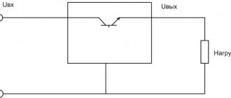
When you and I, my friends, have figured out what this transistor is, let's find out how it works. It is designed quite simply, you just need to understand the principle. To do this, we introduce two very important concepts: emitter and collector. The emitter (as in the word emission) releases charges and they move towards the collector. So, in a state of rest, when, roughly speaking, everything is turned off, no current flows in the transistor, because there is a semiconductor junction between the emitter and the collector. However, when a small voltage is applied to the base of the transistor, the current begins to flow and it can even be amplified. How? Oscillations of a small current are exactly repeated, but with a larger amplitude. Here is a circuit diagram of a simple transistor:
AMATEUR RADIO DIAGRAMS
Here are diagrams for beginners, radio amateurs, recommended for a successful start.
When assembling the proposed circuits, pay special attention to the serviceability of the radioelements used!!!
- Light dynamic devices.
- Sound generators, simulators.
- Power supplies.
- Amplifiers.
DYNAMIC LIGHT DEVICES
Flasher with one LED
Description of the scheme
This circuit is a simple single-ended multivibrator, which causes the LED to glow intermittently. The LED flash frequency is determined by the multivibrator generation frequency. When the power source is turned on, the collector current of transistor VT 2 will change abruptly from zero to the initial value, which is determined by resistors R 1, R 2 and the coefficient h 21e of transistors VT 1, VT 2. The strength of the initial collector current VT 2 is set by selecting resistor R 2, with capacitor C 1 disconnected. In this case, the LED should not light up yet. The selection begins with the resistance values R 1, at which the LED lights up, then the resistance R 1 is increased until the LED goes out. By selecting capacitor C 1, the required blinking frequency is achieved. Resistor values may differ from those indicated in the diagram by +, - 10%. Low-power transistors of the MP group, instead of MP41, you can install MP39, MP42, with any letter index. In place of MP37 you can put MP10, MP38. You can use any commercially available LED. The circuit has been repeatedly tested for functionality and, if assembled correctly, starts working immediately. This circuit can be used as an alarm device, or as an emitter of an alarm device in a car and at home.
Flasher with two LEDs
Description of the scheme
This circuit is a symmetrical multivibrator, the frequency of which depends on the values of capacitors C1, C2, as well as on resistors R 1, R 2. The frequency of alternate blinking of the LEDs, respectively, depends on the frequency of the multivibrator, which in turn can be changed by selecting capacitors C1, C2 and resistors R 1, R 2. Transistors VT 1, VT 2, MP groups and can be MP39, MP40, MP41, MP42, with any letter index. LEDs can be anything except infrared. The circuit is easy to manufacture, has been repeatedly tested for functionality and, if assembled correctly, starts working immediately when power is applied. This circuit can be used as a light indication element in various devices.
SOUND GENERATORS, SIMULATORS
Simple audio frequency generator
Description of the scheme
The generator begins to operate at a voltage of several tenths of a volt, even with a transistor with a low static coefficient. Generation occurs when the S1 button is pressed, due to the action of strong positive feedback between the collector and the base. R1 sets the desired volume and tone of the sound. Transformer T1 - from any transistor small-sized radio receiver. Any high-impedance telephones of the TM-2A type can be used as headphones; in extreme cases, a capsule of the DEM-4M type will also work.
Electronic siren
Description of the scheme
When you press button S 1, capacitor C1 is charged. Capacitor C1 is discharged through a voltage divider on resistors R 2, R 3 connected to the base circuit of transistor VT 1. Since the voltage on capacitor C1 drops as it is discharged, the bias voltage at the base of transistor VT 1 decreases, resulting in a change in frequency sound. A sound reminiscent of a serena's howl is heard from the dynamic head. Transistor VT 1 can be replaced with KT315, KT3102 with any letter index. Transistor VT 2 can be replaced with KT837 with any letter index. When assembling the circuit, pay special attention to the correct connection of the button. Despite the simplicity of the circuit, for some reason, it is the connection of the button that is often confused; as a result, serenading does not simulate, but only a normal sound tone of a certain frequency is heard. The circuit has been repeatedly tested for operability, and with the ratings of the radio components indicated in the circuit and error-free assembly, it begins to work immediately.
Two tone call
Description of the scheme
The bell consists of two generators, a tone generator made on transistors V 3, V 4 and a symmetrical multivibrator V 1, V 2. As is known, when a multivibrator is operating, its transistors alternately close and open. This property is used to control the frequency of the tone generator. The output of the multivibrator is connected to the tone generator through resistor R 5, so it will periodically be connected to the common wire (to the plus of the power source), i.e. parallel to resistor R 7. In this case, the frequency of the generator will change abruptly; when the transistor from the dynamic head B 1 is closed, the sound of one tone will be heard, and when open, another tone will be heard. Capacitors C2, C3 protect the multivibrator from pulses penetrating from the tone generator. In the absence of capacitors, the frequency of the multivibrator will change, which will lead to the appearance of unpleasant tones in the ringing sound. In place of those indicated in the diagram, you can use any other low-power low-frequency germanium transistors of the appropriate structure. Capacitors may differ from the nominal value indicated in the diagram by +.- 10%. Any dynamic head B1, with a power of 1-2 W. and a voice coil DC resistance of 4-10 Ohms. In place of capacitors C2, C3, you can install one electrolytic non-polar capacitor of 1.2 microfarads. for a rated voltage of at least 6V. The bell parts can be mounted on a printed circuit board made of foil getinax or fiberglass. The circuit has been repeatedly tested for operability; with the ratings of the radioelements indicated in the circuit and error-free assembly, it does not require adjustment.
PCB drawing
Telegraph simulator on IC K155LA3
Description of the scheme
The proposed telegraph simulator is quite simple to manufacture and is intended for independent study of the telegraph alphabet. The S1 button is a mechanical telegraph key. The device consists of 4 2I elements - NOT the K155LA3 microcircuit. Elements DD1.1, DD1.2, DD1.3 form a pulse generator with a frequency of 1000 Hz. Element DD1.4 is a buffer. Using resistor R1, the frequency of the generator is adjusted. The power source can be a low-power 5V power supply.
POWER SUPPLIES
Simple regulated power supply
Transistor-based designs require a constant voltage of a certain value for their power supply, 1.5 V, 3 V, 4.5 V, 9 V and 12 V. So that when checking and setting up assembled circuits, you do not waste money on purchasing galvanic cells and batteries, use a universal power supply that runs on AC power and allows you to get any DC voltage. The diagram of such a block is shown in the figure. Its output voltage can be smoothly varied from 0.5 to 12 V. Moreover, it will remain stable not only when the mains voltage changes, but also when the load current changes from several milliamps to 0.3 A. In addition, the power supply is not afraid of short circuits in the load circuit, which are not uncommon in the practice of radio amateurs.
Let's take a closer look at the operation of the power supply. It is connected to the network using a two-pole plug XP1. When the contacts of switch SA1 are closed, the mains voltage is supplied to the primary winding of the step-down transformer T1. An alternating voltage appears at the terminals of the secondary winding, significantly less than the mains voltage. It is rectified by diodes VD1 - VD4, connected in a so-called bridge circuit. To ensure that the rectified voltage is as stable as the voltage of the battery of galvanic cells, there is a large-capacity electrolytic capacitor C1 at the output of the rectifier. The rectified voltage is supplied to several circuits: R1, VD5, VT1, R2, VD6, R3; VT2, VT3, R4, (R2, VD6) is a zener diode with a ballast resistor. They make up a parametric stabilizer. As we said above, regardless of the fluctuations in the rectified voltage on the zener diode VD6 there will be a strictly defined voltage equal to the stabilization voltage of this type of zener diode (in our case from 11.5 to 14 V). A variable resistor R 3 is connected in parallel with the zener diode, with the help of which the desired output voltage of the power supply is set. The closer the resistor slider is to the top terminal, the greater the output voltage. From the variable resistor motor, voltage is supplied to the amplifier stage assembled on transistors VT2 and VT3. We can think of it as a power amplifier that provides the required current through the load at a given output voltage. Resistor R5 simulates the load of the power supply when nothing is connected to the XT1 and XT2 terminals. The voltage on it is almost equal to the voltage between the variable resistor motor and the common wire (XT2 terminal). To be able to control the output voltage, a voltmeter consisting of a microammeter and an additional resistor R 6 is introduced into the block.
Note: Rectifier diodes of the diode bridge VD1 - VD4 can be replaced with more modern types KD226 which are designed for a reverse voltage of more than 250V or imported analogues. Transistors VT1, VT2 can be replaced with KT361 or imported analogues. The VT3 transistor can be replaced with a KT837 with any letter, which will even facilitate its installation on the heat sink. A duralumin or aluminum plate 2mm thick, 40mm wide, 60mm high is suitable as a heat sink. The installation of radioelements is carried out on a printed circuit board made of fiberglass, although there are examples that at first the circuit board was made of thick cardboard. The entire structure is placed in a housing made of dielectric material (plastic, plastic, etc.).
Mounting transistor VT3 on the heat sink.
When assembling you need to be careful and careful because... here on the primary winding of the transformer there is a life-threatening voltage of 220V.
AMPLIFIERS
Scheme of a transformerless push-pull ULF
Description of the scheme
A simple transformerless push-pull amplifier with a power of 1.5 W. The high-frequency transistor P416 is used here for the reason of reducing the noise of the input stage as much as possible, because in addition to being high-frequency, it is also low-noise. In practice, it can be replaced with MP39 - 42, with a deterioration in noise characteristics, respectively, or with silicon transistors KT361 or KT3107 with any letter. letter, due to which a bias voltage is formed at the bases of the transistors. The voltage at the midpoint (the negative terminal of capacitor C2) will be equal to 4.5V. It is installed by selecting resistors R2, R4. The maximum permissible operating voltage of capacitor C2 can be 6V.
Material from the site https://www.lessonradio.narod.ru
What are the differences between different transistors?
Using a simple transistor as an example, we analyzed its operating principle, but there are a great many of them. Let's learn to distinguish them and find out why each of them is needed.
Bipolar
Bipolar transistors are the most popular. In a semiconductor, such transistors have two pn junctions. Charge is transferred through them by holes and electrons.
Among them, there are also several subtypes (they depend on the location of the transitions and the number of electrodes), including:
- compound transistor pnp type;
- composite transistor npn type;
- more complex multielectrode ones (there can be 2 emitters at once);
- heterojunction transistors.
Avalanche transistors
This is a truly interesting type of transistor because it works very efficiently and at the same time very quickly. Their main advantages are high operating voltages and, of course, turn-on speed, and this is very important in electronics. Scientists are still puzzling over how to use these transistors with maximum efficiency, although they are still showing amazing results.
Unijunction transistors
There are such transistors in the world. There is only one transition, so the classification is much simpler:
- the first type is with a “p” base;
- and the second one is with “n” base.
Transistors with control junction
This is also a very interesting and unusual type of transistor, because, as the name suggests, it has a controlled transition, which makes it even more universal, but also makes it more expensive. We will not dwell on the subspecies, as they are all approximately the same as the previous ones.
Insulated Gate Transistors
And what kind of shutter is this, you might think. I'm telling you. As I wrote above, the transistor starts working when a small voltage is applied to it. So, the electrode to which voltage is applied is called a gate. There is nothing special here, it’s just that the gate itself is isolated, which gives more opportunities to control the transistor and for some tasks this is indeed very useful.
Now that we know quite a lot about transistors, we invite you to delve into history and find out how that Darlington transistor came to be.
DIY transistor audio amplifier circuit
The range of sound frequencies that are perceived by the human ear is in the range of 20 Hz-20 kHz, but a device made on a single semiconductor device, due to the simplicity of the circuit and the minimum number of parts, provides a narrower frequency band. In simple devices, a frequency range of 100 Hz-6,000 Hz is sufficient for listening to music. This is enough to play music on a miniature speaker or earphone. The quality will be average, but quite acceptable for a mobile device.
The circuit of a simple audio amplifier using transistors can be assembled using silicon or germanium products of direct or reverse conduction (pnp, npn). Silicon semiconductors are less critical to supply voltage and have less dependence of characteristics on junction temperature.
The history of transistors
At the dawn of the past centuries at the end of the 19th century, physicists and practitioners (Guthrie, Brown, Edison, Bowes, Picard, Fleming) from different countries made a fundamental discovery and received patents for a “detector”, “rectifier” - that’s what the diode was called then. The diode was followed by the epoch-making discovery of the transistor. Listing the names of scientists from different countries who put their head and hands to the discovery of the transistor would take many lines.
The main theorists are Shockley, who worked at Bell Telephone Laboratories, as well as his colleagues Bardeen and Brattain.
From left to right: Shockley, Bardeen and Brattain
As a result of their work, in 1947, the first sample of a working point-type germanium transistor was obtained, and on its basis, in the same year, the first amplifier was developed, which had a gain of 20 (10 times) at a frequency of 10 MHz.
Serial production of point-point transistors by Western Electric began in 1951 and reached about 10,000 units per month in 1952. In the USSR, the first point-point transistor was created in 1949. Serial production of point-point transistors was launched in 1952, and planar transistors in 1955. This was followed by the following discoveries in theory and technology: transistors based on grown junctions (1950), alloy transistors (1952), diffuse meta-transistors (1958), planar transistors (1960), epitaxial transistors (1963) .), multi-emitter transistors (1965), etc.
How did our hero, the Darlington transistor (hereinafter referred to as TD), appear among them? Darlington is a city in the UK. However, people can also have surnames based on cities or vice versa. This is an employee of the same Bell company - Sidney Darlington
Sydney Darlington
An article about the Darlington transistor in English. language can be read here.
Why was this “sweet couple” needed? The fact is that the first transistors had very mediocre characteristics, if you look at today's successes. First of all, the gain is low. Now this seems strange - just think, a cascade connection is elementary! But then, in 1953, this was pioneering work.
Serial connection of transistors
During operation of the power transistor, a voltage drops at its collector-emitter junction, which is the difference between the input and output voltages. In some cases, this difference may exceed the maximum permissible collector-emitter voltage of the transistor available. In this case, it is necessary to use a series connection of several transistors.
Circuit for sequential connection of transistors
An equivalent transistor would have the following parameters:
To balance the voltages that will drop at the collector-emitter transition of transistors, balancing resistors R1 and R2 resistance are introduced, which can be determined by the formula
where IB is the base current of the composite regulating transistor.
Theory is good, but without practical application it’s just words. Here you can do everything with your own hands.
Source
Transistor parameter designations
Let's agree on the designations of certain parameters, abbreviations that we will need when discussing, calculating and modeling circuits. For this we will use the designations generally accepted in datasheets (datasheet - technical description or passport for a radio element).
Abbreviations:
Basic parameters of the transistor according to the datasheet:
Parameters (set, measured or calculated):
The simplest key
In the future, we will specifically call a field-effect transistor a MOSFET, that is, field-effect transistors with an insulated gate (aka MOS, aka MIS). They are convenient because they are controlled exclusively by voltage: if the gate voltage is greater than the threshold voltage, then the transistor opens. In this case, the control current does not flow through the transistor while it is open or closed. This is a significant advantage over bipolar transistors, in which current flows the entire time the transistor is open.
Also, in the future we will only use n-channel MOSFETs (even for push-pull circuits). This is because n-channel transistors are cheaper and have better performance.
The simplest switch circuit using a MOSFET is shown below.
Again, the load is connected “from above”, to the drain. If you connect it “from below”, the circuit will not work. The fact is that the transistor opens if the voltage between the gate and source exceeds the threshold. When connected “from below,” the load will produce an additional voltage drop, and the transistor may not open or not open completely.
Despite the fact that the MOSFET is controlled only by voltage and no current flows through the gate, the gate forms a parasitic capacitor with the substrate. When the transistor turns on or off, this capacitor is charged or discharged through the input of the switch circuit. And if this input is connected to the push-pull output of the microcircuit, a fairly large current will flow through it, which can damage it.
With push-pull control, the capacitor discharge circuit actually forms an RC circuit in which the maximum discharge current will be equal to
where is the voltage that controls the transistor.
Thus, it will be enough to install a 100 Ohm resistor to limit the charge and discharge current to 10 mA. But the greater the resistance of the resistor, the slower it will open and close, as the time constant will increase. This is important if the transistor switches frequently. For example, in a PWM controller.
The main parameters that you should pay attention to are the threshold voltage, the maximum current through the drain and the drain-source resistance of an open transistor.
Below is a table with examples of characteristics of MOSFETs.
| Model | |||
| 2N7000 | 3 V | 200 mA | 5 ohm |
| IRFZ44N | 4 V | 35 A | 0.0175 Ohm |
| IRF630 | 4 V | 9 A | 0.4 ohm |
| IRL2505 | 2 V | 74 A | 0.008 Ohm |
Maximum values are given for. The fact is that for different transistors, even from the same batch, this parameter can differ greatly. But if the maximum value is, say, 3 V, then this transistor is guaranteed to be used in digital circuits with a supply voltage of 3.3 V or 5 V.
The drain-source resistance of the above transistor models is quite small, but it should be remembered that at high voltages of the controlled load, even this can lead to the release of significant power in the form of heat.
Transistor Basics
What can we say here that is new? Never mind! But it's still useful to review the basics, isn't it? 
Basic dogmas about the bipolar transistor:
- A transistor is a current device. The base current is controlled by the collector current.
- The transistor has only three terminals. Base (B), collector (K) and emitter (E) and, respectively, in English. B (Base), C (Collector), E (Emitter).
- The emitter current is the sum of the collector and base currents. IE = IK + IB
- The current gain in a circuit with OE is the ratio of the collector current increments to the base current. h21e (β)=ΔIK / ΔIБ.
- h21e depends on the collector current. At its minimum or maximum values, h21e tends to zero.
- At the input (with reverse voltage), the transistor resembles a diode in direct connection.
- At the input (with reverse voltage), the transistor resembles a zener diode.
- The transistor in the closed state still gives in and gives off leakage current.
- A transistor base that is not connected anywhere and hangs in the air is its death. Therefore, it is imperative to connect the base to ground through a high-resistance resistor.
- The transistor in the open state will provide a non-zero voltage drop at the Base-Emitter junction and it will be approximately hundreds of milliVolts, or more precisely from 0.5-0.7 Volts.
- The transistor does not like high frequencies. You know, all sorts of Miller effects and stuff.
- For high load power, the transistor housing is made in a certain way so that it can be placed on a radiator
- The safe operating area (OSR) is all transistor limitations when combining the maximum current and voltage
- Minimum transistor noise is achieved at minimum optimal collector currents
- The maximum performance of the transistor is achieved at maximum optimal collector currents.
Great! Having learned a lot about the history of transistors and refreshed the basics of transistors in our heads, we return to the Darlington transistor, because we still do not understand why it is so remarkable.
Disadvantages of the Darlington scheme
Unfortunately, that's where the benefits end. The first drawback of this circuit is that the voltage at the emitter base is twice as high. Here we are dealing with a series connection of base-emitter junctions, so the voltages on each of them add up (about 0.7 V when turned on).
| This means that the UBE of the Darlington circuit is approximately 1.4 volts. This should be taken into account when choosing base current limiting resistors. |
However, a much more serious disadvantage is the increased saturation voltage. This issue is best analyzed using a voltage recording diagram.
Voltage distribution in a saturated Darlington transistor
The collector-emitter voltage of a Darlington transistor consists of:
- base-emitter voltage of transistor T2,
- collector-emitter voltage T1.
When the system is saturated, transistor T2 should still be on, that is, its base-emitter voltage is 0.7 V. Due to this, transistor T1 can saturate properly and its U CE drops to an arbitrary level of 0.2 V. After summation These voltage values, it turns out that U CE of transistor T2 is as much as 0.9 V!
| This voltage loss must be taken into account when designing the circuit because it is definitely not a value that can be neglected! |
In our example circuit from the beginning of this article, a single transistor has a big advantage: in a saturated state it will have about 0.2 V (in practice a little more), which, combined with the 5 A current flowing through the collector, will lead to power dissipation about 1 W.
This amount of heat can be easily dissipated using a small radiator, that is, an element that removes heat. It is usually made of aluminum, which is lightweight and conducts heat well. Radiators have different shapes - most often in cross section they resemble a comb, increasing the surface of contact with the flowing air.
Radiator - heat sink element
But let's get back to controlling our engine. If we use Darlington, this power will be wasted, and we will need a much stronger radiator. In addition, the receiver supply voltage will be lower by about 1 V. In the case of circuits powered from a low voltage, such as 3.3 V, this will be a significant reduction.
| 5 W is a lot of power. 5 W, for example, can be consumed by an LED table lamp. |
And also, in a clogged state, the collector-emitter voltage of both transistors is almost the same. This means that when driving the receiver from a power source, for example 60 V, both transistors must withstand this voltage (with a margin).
First about why compound
As you already understand, the transistor was invented by the engineer Darlington, but in the end this invention received a double name. On the one hand, it is a Darlington transistor, but on the other hand, it is a composite transistor. So why composite? After all, when we talked about species, there was no talk about any components. It's simple, my friends. Darlington decided to use 2 bipolar transistors at once. They were implemented on one crystal made of silicon and there, naturally, were 2 transitions. In the West, they are used to calling this invention a Darlington transistor, but in our country it is simply called a composite one. Well, let's find out even more about him.
Board mounting
To give a single-transistor single-band receiver with a continuously adjustable variable capacitor a constructive appearance, mount it on a board made of sheet metal, textolite or vinyl plastic with a thickness of 1.5...2 mm (Fig. 4). Approximate dimensions of the board: width .80...65 mm, length 120... 150 mm.
The free space on the board will later be occupied by parts of the bass amplifier. As mounting posts for resistors and capacitors, use pieces of wire with a diameter of 1...1.5 and a length of 8...10 mm, driving them into the holes in the board (Fig. 4). Make connections between mounting posts with conductors from the bottom of the board and be sure to solder them: reliability of contacts at the connection points is ensured only by soldering.
Rice. 4. Installation of the receiver circuit on the board, soldering of parts.
After finishing the installation, check (using the schematic diagram of the receiver) for errors, unreliable contacts, or short circuits between exposed conductors. If everything is in order, then connect the antenna and grounding, turn on the power and listen to the entire range of waves covered by the receiver.
So what's so special about this?
In order to understand the main advantages of a composite transistor, you need to remember why a transistor is needed in the first place. Of course, it also increases the current. And each transistor has its own gain, that is, how many times the current is amplified by a given transistor. So, let’s imagine that for one transistor this number is 60, and for the other 100. I note that each new transistor does not add the coefficient, but multiplies it, which means that in the end we will get a final force of 6000 and this is much more than the figure.
Parallel connection of transistors
Modern transistors make it possible to implement electronic circuits designed for wide ranges of changes in currents and voltages, but in some cases, parallel connection of transistors is used to increase the permissible power dissipation.
Transistor parallel circuit diagram
The maximum permissible current flowing through such a composite transistor is:
With such a circuit for connecting transistors, it should be taken into account that due to the spread of parameters of parallel-connected transistors, the currents are distributed unevenly between them. Most of the current will flow through the transistor, which has a higher gain. The power dissipated by transistors can be equalized by including additional balun resistors with low resistances in their emitter circuits. Since in practice it is difficult to select such resistances for each transistor, in practical circuits resistors of the same resistance are placed in the emitters of all transistors. The resistance of the balancing resistors R1 and R2 can be determined by the formula
where n is the number of parallel connected transistors
IK is the current passing through the collector.
This method is associated with a deterioration in the amplification properties of transistors, but its advantage is the possibility of obtaining a powerful power element using relatively low-power transistors.
Even this can still be improved
One not very famous engineer, calling himself Siklai, saw how a compound transistor worked and was very impressed. At first, he thought that this was truly the limit of perfection, but one day an insight came to him and he figured out how to make this device even more effective. The resulting transistor was called a complementary Darlington transistor. It consists of bipolar transistors of different conductivities. What does this give? Sometimes this helps increase the gain even further, which is exactly what you need. Here, take a look at the diagram:
Two-stage ultrasonic amplifier using transistors of different structures
It is designed with direct coupling between stages and deep negative DC feedback, which makes its mode independent of ambient temperature. The basis of temperature stabilization is resistor R4, which works similarly to resistor R3 in the previous design
The amplifier is more “sensitive” compared to a single-stage amplifier - the voltage gain reaches 20. An alternating voltage with an amplitude of no more than 30 mV can be supplied to the input jacks, otherwise distortion will occur, which can be heard in the headphone.
They check the amplifier by touching the input jack X1 with tweezers (or just a finger) - a loud sound will be heard in the phone. The amplifier consumes a current of about 8 mA.
Rice. 2. Diagram of a two-stage AF amplifier using transistors of different structures.
This design can be used to amplify weak signals, such as from a microphone. And of course, it will significantly enhance the signal 34 removed from the load of the detector receiver.
Pros and cons of a composite transistor
If we talk about the advantages of this wonderful device, then this is, of course, a very high gain, which allows you to run the transistor even with a very low base current. However, there are also disadvantages, as always. It would seem that this might not be the case here, but it might be. The fact is that there is no smell of performance here, so the Darlington transistor is mainly used in low-frequency circuits. Usually they are installed on the output stages of circuits, as well as in electric motor control units - there they really have their place. Also, many modern cars cannot do without them, because they are the most important part of the electronic circuit switch in the ignition system.
This is the circuit that radio amateurs use when they make a compound transistor with their own hands (using a Darlington transistor together with an electric motor):
Circuit of a simple audio amplifier using one transistor
It is almost impossible to obtain good electrical characteristics in an amplifier assembled on one semiconductor, so high-quality devices are assembled on several semiconductor devices. Such designs produce tens and hundreds of watts at low-impedance loads and are intended for operation in Hi-Fi complexes. When choosing a device, the question may arise as to which transistors can be used to make a sound amplifier. These can be any silicon or germanium semiconductors. ULFs assembled on field-effect semiconductors have become widespread. For low-power devices with low-voltage power supply, you can use silicon products KT 312, KT 315, KT 361, KT 342 or germanium products of the old MP 39-MP 42 series.
A do-it-yourself power amplifier using transistors can be made using the complementary pair KT 818B-KT 819B. This design will require a pre-block, an input stage and a pre-final block. The pre-assembly includes signal level control and tone control for high and low frequencies or a multi-band equalizer. The voltage at the output of the preliminary unit must be at least 0.5 volts. The input node of the power block can be assembled on a high-speed operational amplifier. In order to pump up the final part, you will need a pre-terminal cascade, which is assembled on a complementary pair of medium-power devices KT 816-KT 817. The designs of powerful low-frequency amplifiers are distinguished by complex circuitry and a large number of component elements. To properly adjust and configure such a unit, you will need not only a tester, but an oscilloscope and an audio frequency generator.
The modern element base includes powerful MOSFET devices that allow the design of high-class ULFs. They provide signal reproduction in a frequency range from 20 Hz to 40 kHz with high linearity, a non-linear distortion factor of less than 0.1% and an output power of 50 W and above. This design is easy to replicate and adjust, but requires the use of a high quality bipolar power supply.
Let's compare a compound transistor and a push-pull one
Consider the previous circuit, which uses a compound transistor. If a current of 1 mA is applied to the base, then this circuit will amplify it 1000 times, and as a result, a current of 1000 mA will flow to the collector. I note that instead of an electric motor, we can connect both a relay and a light bulb, for example, and with the help of them we can already switch large loads.
What if we put a simple Darlington transistor into the transistor of the engineer Sziklai? Then we will have something like a push-pull amplifier. This is so because only one of the two transistors can be open at a time. Composite transistor circuit:
Here the input voltage will be inverted and the output will be reverse to the original voltage. In order to make the circuit more universal, an inverter is usually installed at the input. Thus, the current is inverted 2 times.
Push-pull AF power amplifier using transistors
It is made on transistors of different structures and has a voltage gain of about 10. The highest input voltage can be 0.1 V.
The first two-stage amplifier is assembled on transistor VT1, the second is assembled on VT2 and VT3 of different structures. The first stage amplifies the signal 34 in voltage and both half-waves are equal. The second one amplifies the signal by current, but the cascade on transistor VT2 “works” at positive half-waves, and on transistor VT3 at negative half-waves.
Rice. 4. Push-pull AF power amplifier using transistors.
The direct current mode is chosen such that the voltage at the point of connection of the emitters of the transistors of the second stage is equal to approximately half the voltage of the power source.
This is achieved by turning on the feedback resistor R2. The collector current of the input transistor, flowing through the diode VD1, leads to a voltage drop across it. which is the bias voltage at the bases of the output transistors (relative to their emitters), it allows you to reduce distortion of the amplified signal.
The load (several parallel-connected headphones or a dynamic head) is connected to the amplifier through an oxide capacitor C2.
If the amplifier will operate on a dynamic head (with a resistance of 8 - 10 Ohms), the capacitance of this capacitor should be at least twice as large. Pay attention to the connection of the load of the first stage - resistor R4. Its upper pin in the circuit is not connected to the power supply positive, as is usually done , and with the lower load terminal.
This is the so-called voltage boost circuit, in which a small positive feedback voltage is supplied to the base circuit of the output transistors, equalizing the operating conditions of the transistors.
Where else is a compound transistor used?
Very often a compound transistor is used with a Szyklai transistor paired in one circuit. For example, 2 electric motors in many VCRs were controlled by these transistors.
Also based on the Darlington circuit, the ULN2003A microcircuit was created, which is often used in amateur radio assemblies.
You can also watch a video where they talk in detail about composite transistors:
Composite transistor. Schemes of Darlington, Siklai. Calculation, application
Composite transistor, Darlington circuits, Sziklai.
Calculation, application Composite transistor
used if a very high current transfer coefficient (h) is required. For a composite transistor, h is equal to the product of the h transistors included in its composition.
The use of a composite transistor requires careful selection of transistor operating points and calculation of parameters. The formulas are given in the article.
Composite transistors are used where it is necessary to control large currents with a very small current, that is, where a large current transfer coefficient is required. However, the compound transistor has some significant disadvantages that limit its use. The compound transistor is widely used in analog circuits. Its use in key schemes is not effective.
Features of the device
For composite transistors, the gradual decrease in voltage along the conductor at the base-emitter junction is twice the standard. The level of voltage reduction across an open transistor is approximately equal to the voltage drop that the diode has.
According to this indicator, a composite transistor is similar to a step-down transformer. But relative to the characteristics of the transformer, the Darlington transistor has much greater power gain. Such transistors can operate switches with a frequency of up to 25 Hz.
The system for the industrial production of composite transistors is set up in such a way that the module is fully equipped and equipped with an emitter resistor.
Sziklai pair and cascode circuit
Another name for a compound semiconductor triode is a Darlington pair. In addition to her, there is also a couple of Siklai. This is a similar combination of a dyad of basic elements, which differs in that it includes different types of transistors.
As for the cascode circuit, this is also a variant of a composite transistor, in which one semiconductor triode is connected according to a circuit with an OE, and the other according to a circuit with an OB. Such a device is similar to a simple transistor, which is included in a circuit with an OE, but has better frequency characteristics, high input impedance and a large linear range with less distortion of the transmitted signal.