Progress, as we know, does not stand still. Especially in electronics. In our times, when you can easily fit half a computer on a square centimeter of a board, and special programs allow you to virtually “test” the developed device without ever picking up a soldering iron and a tester, this article may seem hopelessly outdated. But who knows - maybe it will be useful for some beginners.
Well, let the experienced ones perceive this text as another tale about how the surviving radio destroyers live in the remote wilderness (the Far East, very distant), where I think civilization will not reach very soon.
Etching circuit boards with hydrogen peroxide and citric acid
Author: Vladimir Vasiliev · Published on May 9, 2022 · Updated on August 25, 2018
Hello dear friends! It’s 5:30 in the morning, today I woke up early on purpose to write something useful. And yes, today is May 9 on the calendar, so I congratulate you on this great day, Happy Victory Day!
Today we will talk about a solution for etching printed circuit boards, which is striking in its accessibility and simplicity. Yes, today we’ll talk about how you can etch a board using hydrogen peroxide and citric acid and a little salt.
What etching solutions are there?
There are many different solutions for etching printed circuit boards, including popular etching mixtures and some that are not particularly popular.
In my opinion, the most popular etching solution in the amateur radio community is ferric chloride. I don’t know why this is so, maybe it’s a conspiracy of radio store sellers who specifically offer ferric chloride and tactfully keep silent about alternatives. But there are alternatives:
- Etching with copper sulfate and salt
- Ammonium persulfate etching
- Sodium persulfate etching
- Etching with hydrogen peroxide and hydrochloric acid
- Etching with hydrogen peroxide and citric acid
If you have other options for etching solutions, I would be grateful if you share them in the comments to this post.
It depends on you, but my least favorite process in the manufacture of printed circuit boards is their etching. It doesn’t seem to be that complicated - I threw the board into a water bottle with ferric chloride, took it out after half an hour, washed it and it’s done. But storing and constantly pouring this LIQUID from a bottle into a bath is fraught with staining everything around: from hands and clothes, to walls, floor, table, cat... well, you get the idea. In general, it is better to do this dirty business in a specially designated place. Or switch to less dirty components, which is what I decided to try to do. Therefore, now we will consider the two most popular and cleaner compositions for etching printed circuit boards.
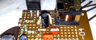
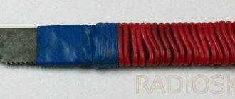
I just needed to etch three small single-sided boards, the pattern was transferred using LUT, roads 0.4 mm thick
1. Hydrogen peroxide + citric acid + table salt
This recipe is new and was first published here . This is probably the most affordable option for etching printed circuit boards; components can be easily obtained at the nearest pharmacy or store. The price of a 100 ml bottle of hydrogen peroxide is about 10 rubles; for an 80 gram package of citric acid I paid 23 rubles. And if you go to wholesale stores, you can generally buy citric acid for 100 rubles/kg, although in bags of 25 kg.
To prepare a solution, 30 grams of citric acid and a teaspoon of table salt are dissolved in 100 ml of 3% peroxide.
This volume, according to the author of the recipe, is enough to etch copper with an area of 100 cm2, but more often you have to prepare more solution, depending on the etching utensils and the dimensions of the board. The downside is that the solution cannot be stored for a long time, and if the boards are etched rarely, you will have to prepare the solution anew each time. At my place, I mixed 200 ml of peroxide, 80 grams of citric acid and two teaspoons of table salt.
2. Ammonium persulfate
This is also a relatively new method of etching, and we have only recently started selling jars of persulfate in radio stores. According to reviews from those who have already tried this method, it poisons well and, most importantly, does not leave walls and floors stained with rust, as ferric chloride likes to do. For a jar of persulfate weighing 250 grams I paid 150 rubles. According to the instructions, this volume is dissolved in 0.5 liters of water; after etching, the finished solution can be stored and reused.
The first two compositions turn out to be equally transparent and etching for both occurs with active gas formation. If you etch the board with the foil facing down, you will have to shake it from time to time to shake off bubbles from the surface.
When etching in persulfate, one unpleasant feature emerged: in addition to bubbles, some kind of hard transparent coating forms on the copper. Judging by the reaction formula below, the transparent coating is the ammonium salt of sulfuric acid (ammonium sulfate)
(NH4)2S2O8 +Cu → CuSO4 + (NH4)2SO4
This plaque is quite difficult to scrape off and naturally, the copper underneath stops being etched. I had to often take out the board and clean the copper from plaque, otherwise the board would be etched in pieces. I don’t know why this happens, no one has complained about it, perhaps this happens while the solution is fresh and the reaction is too intense. I'll see how the next boards are etched in the same solution.
3. Ferric chloride
And since I started comparing, I took a can of XJ at the same time. A method familiar to everyone who has made printed circuit boards at home. Knowing about the amazing ability of ferric chloride to spread everything around, I really didn’t want to even open a jar of this crap. But it was still interesting to visually compare the two new methods with what I have been using to etch boards for the last 10 years.
250 gr. a jar of HJ cost 120 rubles
For a small board, just a little solution is enough. Ferric chloride is good because it is easy to dose according to the color of the resulting solution; it should be the color of strong tea.
All three compositions begin to etch faster if you heat them to a temperature of 35-40 degrees, this can be done, for example, by placing the dishes in a basin or sink with hot water. In hydrogen peroxide and persulfate it is very good to observe the process, the compositions are transparent and you don’t have to take out the board to see how much unetched copper is left.
During the etching process, the color of the peroxide solution first turns green and then becomes increasingly blue. The color of the persulfate also changes to blue and the longer the etching goes on, the more saturated the color becomes. And the slurry with ferric chloride remains rusty in color, becoming darker 
Results
Copper in the solutions considered is etched quite quickly. We had to keep the board in ammonium persulfate for the longest time, because we had to take the board out and remove plaque from the surface of the copper. In total, etching in peroxide took 15 minutes, in ferric chloride about 20 minutes, and in ammonium persulfate a little more than 30 minutes.
At first glance, all three boards were well etched, but when I washed them, it turned out that persulfate had gotten under the toner and eaten up half of the tracks! This is something I definitely didn’t expect.
In hydrogen peroxide (board on the left), as well as in ferric chloride, there are no such tricks. Although peroxide still produces a better result - the edges of the tracks, if you can see, are smoother (all three boards were rolled simultaneously on a laminator and from the same sheet, so we do not take into account factors such as the quality of rolling toner onto copper, it is the same for all three) .
To make the experiment complete, I decided not to pour out the solutions with peroxide and persulfate. I wonder if the peroxide will poison at least a month after mixing. Yes, and you need to achieve a suitable result from persulfate.
* * *
So, after a long pause of 2 months, I took out both solutions. They were kept under the bathroom, where it was dark and cool. I did not pour the solutions, I stored them directly in flasks, covering them with a rubber glove, in case the solutions began to release gas (I heard stories about jars in which the persulfate solution was stored that exploded). I did not observe any gas formation during storage, but a sediment containing persulfate formed at the bottom. The color of both solutions evened out and they became similar, if not for the sediment it would have been difficult to distinguish which was which.
And here is the sediment at the bottom of the ammonium persulfate solution. Blue crystals, Heisenberg would approve :) Or maybe not blue, but still beautiful in person.
I prepared two boards that the persulfate solution ruined for me last time (these are boards for a small amplifier based on the LM4871 chip)
The ammonium persulfate solution immediately got to work and began to etch the board with strong release of gas bubbles.
But the hydrogen peroxide solution, unfortunately, ran out of steam. He couldn't do anything other than lighten the copper on the board a little. The solution had to be poured out and etched in persulfate.
And this time there were no etched paths
In general, I was very pleased with the two new lineups. If ammonium persulfate is available in stores, it will be a good replacement for ferric chloride, although the difference in price is small. For better results, it would be a good idea to assemble an etching bath with rotaspray . Then the undercutting won’t be a problem and you can make the roads much thinner (again, without fear that they will end up at 0).
Well, as for the hydrogen peroxide solution, it is well suited for the role of auxiliary. In case you run out of persulfate, you can always mix peroxide with lemon; fortunately, these components are used in everyday life and can almost always be found in the kitchen cabinet or in the nearest store.
What are the disadvantages of etching in ferric chloride?
Ferric chloride solution is good for everyone, it is not difficult to prepare and the etching process usually goes quickly. When preparing, it is very easy to figure out the concentration, which is called “by eye”. Once prepared solution is enough for dozens of circuit boards. But it has some disadvantages that are very annoying:
- The solution is not transparent, which makes it difficult to control the process. You have to constantly remove the board from the etching solution.
- Ferric chloride solution stains plumbing fixtures very badly. Each board etching session ends with the process of scraping off the plumbing fixtures (sink, bathtub, and anything else the solution might come into contact with).
- It stains clothes very much. When working with ferric chloride, you should wear clothes that you wouldn’t mind throwing away, because the solution eats into the fabric very strongly, so much so that it is almost impossible to wash it later.
- The solution has an aggressive effect on any metal nearby; even when stored in unsealed containers, nearby metal objects may become rusty. Once I closed a jar of ferric chloride with a metal lid (the lid was painted), after a couple of months this lid turned into dust.
Tips for working with soldered boards
Some useful tips to help you assemble the board correctly:
- Immediately cut the board to the required size. For this, ordinary scissors, a cutter, or a hacksaw are suitable. You can even just break it along the holes, but then clean the edges.
- If you are not going to use the board right now, then do not touch the areas with foil with your hands again. Hands may be wet, which will lead to surface corrosion and poor contact.
- If oxides or dirt occur, clean them with fine sandpaper or a regular eraser.
- Radio elements are installed on the side where there are no foil strips. The leads are inserted into the holes and soldered on the reverse side.
- The blue color of the conductive paths indicates the “minus” of the circuit, the red “plus”, and green is used at your discretion. The tracks are marked on the same side where the foil is located.
- The most important positioning of parts occurs in a vertical position, since in this case an error will lead to an incorrectly assembled chain.
Please note that both types of breadboards may have slots on the sides. This is necessary for those who assemble a large device consisting of several modules. The grooves allow you to assemble one large board from several small ones.
How to etch boards in hydrogen peroxide and citric acid
Although I have always been an adherent of the conservative path, despite all the advantages of the FeCl3 solution, its disadvantages are gradually pushing me to search for alternative etching mixtures. And so I decided to test the method of etching boards in hydrogen peroxide and citric acid.
On the way home, I went to the grocery store and, in addition to the ingredients for a delicious dinner, grabbed 4 10g packets of citric acid. every. Each bag cost me less than 6 rubles.
I went to the pharmacy and bought a bottle of hydrogen peroxide, it cost me 10 rubles.
I don’t have any project at the moment, so I decided to purely test the method, to understand what the big deal is. I found a scrap of foil PCB in my stash and made a few strokes with a permanent marker. This is a kind of imitation of tracks and copper polygons; it will work quite well for experimental work.
Advantages of etching in hydrogen peroxide and citric acid
From the experience gained, we can conclude that this method, like others, has its pros and cons; it has both its advantages and its disadvantages.
- Easily accessible - all components can be easily found at the nearest pharmacy or grocery store.
- Relatively cheap - all the components for preparing the solution are not expensive, less than 100 rubles. (at the time of writing)
- Transparent solution - the resulting solution is transparent, this simplifies observation and control of the etching process.
- Etching occurs quickly enough and does not require heating
- Doesn't stain plumbing
Purpose and device
The development board for solderless assembly allows you to mount an electrical circuit and run it without using a soldering iron. In this case, you can check all the parameters and characteristics of the future device by connecting measuring and control devices to the board.
A breadboard is a plate made of a polymer material that is a dielectric. Mounting holes are drilled on the plate in a certain order, into which the leads of the parts - components of the future device - should be inserted.
The holes allow the connection of leads with a diameter of 0.4-0.7 mm. They are located on the board, as a rule, with a pitch of 2.54 mm.
To simulate the connections of the component leads to each other, the breadboard has special conductive plates that connect the holes in a certain order.
Typically, these connections are made in groups along the board along its long sides. There may be two or three such rows. These contact groups are used as buses for connecting power.
Between the longitudinal rows, the holes are connected by plates in groups of five. These plates are located in a direction across the board.
Near the holes in the places of future contacts, the current-conducting plates have design features that allow them to clamp and firmly hold the leads of the parts, while ensuring the presence of electrical contact. This is the meaning of installation without soldering.
Quality prototyping boards can be assembled and disassembled while maintaining a strong and reliable connection between parts up to 50,000 times.
Breadboards produced industrially and purchased in a retail chain, as a rule, have a layout of contacts and conductive connections between the holes.
What are the disadvantages
Unfortunately, in addition to all the advantages, this etching method is not without its disadvantages.
Disadvantages of etching in hydrogen peroxide and citric acid:
- Disposable solution - the solution is suitable only for one-time use, i.e. during a chemical reaction occurring in it. It will not be possible to etch many boards; you will have to prepare the solution anew each time.
- Expensive - despite the fact that all the ingredients are cheap, in the long run the solution turns out to be more expensive than the same chlorine jelly. After all, for each new board the solution will have to be prepared anew.
That's basically all the shortcomings. In my opinion, this method of etching boards has the right to life and it will definitely find its supporters and admirers. And in some cases, this method may be the only possible alternative, for example, in a remote village with a pharmacy and grocery store.
And with this I will wrap up. It’s already dawn outside and it’s time to prepare a delicious breakfast.
Food for thought
That's all! A solderless breadboard is a very convenient thing for creating breadboards. However, you should be wary of making more or less serious devices on such a board, even if it is a school project.
The fact is that the connections on a solderless board turn out to be very, very unreliable: jumper wires can easily fall out of their sockets, and the contacts oxidize over time. In addition, we must remember that any connector is a capacitor, and the more there are on the board, the less predictable the result will be. So immediately after mastering solderless breadboards, you should definitely learn how to use a soldering iron!
How have boards been etched in the past?
In the past, making a printed circuit board required a lot of effort. First, the diagram was drawn on paper, then holes were made in the workpiece, after which the tracks were transferred to foil PCB or getinax, using paint and varnish products. After the coating had dried, it was peeled off, and the board was immersed in a container with meadow for etching.
The hardest part was etching the board. Since ferric chloride-based meadow was used for these purposes. In the radio circle, such a remedy was not in short supply, but at home one had to look for an alternative, which most often was copper sulfate.
Processing the board carried another secret: the board was etched unevenly. Some paths were corroded, and in some places the surface was under-etched. All due to the inexperience of the craftsmen or repeated use of the puddle solution.
Printed circuit boards using a laser printer.
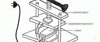
The method of manufacturing single printed circuit boards by transferring a design from a printout on a laser printer is becoming increasingly popular among radio amateurs. It is best to print on thin coated paper - it has less lint, a good result is obtained on sheets of the "Stereo & Video" magazine, as well as "self-adhesive" substrates and thermal paper for faxes (choose the side experimentally). In laser printers, you should enable the maximum toner supply mode (turn off the “economy” mode if it was turned on, set the contrast to maximum, etc.), and also use a path with minimal paper bending (this option is available in older HP LJ 2 models , LJ4, etc.). The board design must be “mirrored”; this option is available in the print menu of many graphics programs, for example Corel Draw, Corel Photo Paint, and when printing from programs that cannot “mirror”, it is necessary to use output to Postscript printers that have a mirroring option in the driver. Instead of outputting to a laser printer, you can use photocopying, but also in maximum contrast mode and onto thermal fax paper. When making two-layer printed circuit boards, to reduce heat shrinkage of the paper, it is recommended to “run” the latter through the printer empty (without printing the image) before printing the image. In addition, both sides should be on the same sheet to avoid severe misalignment due to different heat shrinkage of the paper. The degreased board is laid with the copper side up on a flat surface, with the resulting print on top, toner side down. This “sandwich” is pressed on the paper side with an iron (for 20 - 30 seconds), heated to the ironing temperature of crepe de Chine (ask the ladies). The iron should not immediately melt the image made by the laser printer. That is, the toner at this temperature should turn from solid to viscous, but not liquid. When the board has cooled down, you need to immerse it in warm water and hold it there for several minutes. As soon as the paper becomes limp (it will be visible), everything can be easily pulled off, the rest can simply be rolled up with your finger. Instead of water, you can remove the paper with sulfuric acid. If the tracks are greased, you carelessly removed the iron or placed a cold weight. If the tracks are missing somewhere, the iron is too cold. If the tracks become wide, the iron is too hot, or the board was heated for too long. If the board is double-sided, then first the paper printouts of both sides are aligned, in any free opposite places two technological holes are pierced with a needle, the first side of the board is “ironed” as usual, then it is drilled along the technological holes with a thin drill, and on the other side along them the gap is aligned with the paper printout of the other side. You can poison with ferric chloride (warm it up a little to speed it up) or with hodgepodge with hydropyrite. All this was used even on getinax, there are no peelings of the tracks, tracks up to 0.8 mm wide are normally made, and with some experience up to 0.5 mm. After etching, the toner is removed with acetone, nail polish remover or Flux Off spray. Drilled, trimmed and so on, as usual...
How to etch a board correctly?
To make etching of the board with hydrogen peroxide and citric acid faster, you can use two containers. Simply place the smaller container of meadow into the larger container and pour hot water into it. This will speed up and strengthen the process.
Etching a board in a solution of hydrogen peroxide is done as follows: the board is placed in a meadow with the side on which the tracks are drawn facing down, so that the decomposition products easily sink to the bottom of the container. To ensure the reaction proceeds more evenly, the solution must be stirred lightly from time to time. The whole process takes no more than 10 minutes.
How can you tell if the board has already been etched?
In a hydrogen-acidic environment, the reaction proceeds according to the formula: Cu+ H3Cit +H2O2 → H[CuCit] +2H2O. Etching a printed circuit board in hydrogen peroxide can be considered complete if any reactions in the solution have stopped: it no longer hisses or bubbles.
The finished board is cleaned and washed with water. Toner or paint is washed off with acetone. After which the board is thoroughly wiped and degreased.
Important! Check the tracks for integrity after processing the board. A damaged circuit will not work.
As you can see, etching a board with hydrogen peroxide at home is not only possible, but also safe. It will not be difficult to find the necessary components for preparing the etching composition, and the process itself will take no more than 15 minutes. Today, any radio amateur, thanks to simple and accurate advice, will be able to experiment at home without harming himself or others.
Source
Homemade development board
Very often, when designing electronic circuits, it is necessary to check the correctness of some circuit design solution, and also if you need to debug a circuit, you resort to prototyping it on a breadboard.
Nowadays it is very easy to purchase a special “Breadboard” type development board, which allows you to assemble electronic devices without soldering, simply by inserting the leads of electronic components and jumpers into the sockets of the board.
The name “Breadboard” translates as “board for cutting bread” or “cutting board” - the fact is that since the 1900s, a piece of an ordinary board (on which bread could be cut) has been used as a basis for mounting lamps, transformers and other electronic components when designing various circuits.
More recently, “Breadboard” type boards were practically unavailable; instead, homemade breadboards were used, the components on which were connected by soldering. What kind of boards were used before for prototyping?
There were several types of prototyping technology:
- Installation on the “heels” - here round contact pads were cut out of the fiberglass foil using a special cutter. This technology was mainly used for prototyping or manufacturing permanent circuits operating in the VHF range (excess foil was removed from the board, so the capacitances between pads were small).
- Vertical and horizontal slits were made in the foil fiberglass laminate, and the contact pads were rectangular in shape.
- A wooden board was taken and pushpins were stuck into it, serving as contact pads.
- Holes were drilled in a piece of non-foil fiberglass into which tin contact petals were inserted.
In the first two technologies, parts and wires were soldered directly to fiberglass, which had a bad effect on the service life of these breadboards - due to overheating during soldering, the contact pads often fell off.
Layout with push pins
The technology of prototyping with pushpins in the form of contact pads is the simplest; the buttons are easily serviced using a low-power soldering iron. If the buttons are covered with some kind of decorative coating, they should be sanded before tinning.
The buttons on the board are either arranged in the form of a geometric grid, or are inserted as needed, each time the elements of the circuit are connected. Actually, the ancient “bread cutting board” is the progenitor of this technology - in it, thick copper wires were nailed to wood.
Tin contact petals
The fourth prototyping technology on boards with tin contact petals has been repeatedly described in various literature; let’s consider it in more detail.
The basis of these development boards is non-foil fiberglass, preferably thicker - then the board will be more rigid. If you don’t have non-foil fiberglass on hand, you can use regular fiberglass, after first removing the layer of copper foil from it.
To do this, the foil should be heated over a fire, after which it can be easily separated from the board. You can also use used printed circuit boards by heating the conductors with a soldering iron; they can be removed from the boards by prying them with something sharp.
Then holes with a diameter of 5..6 mm are drilled in the fiberglass (Fig. 1.).
Rice. 1. General view of the breadboard without installed pads and power buses.
Long screws with nuts are installed in the corners of the breadboard to serve as supports. To make contact pads and conductors, tin from condensed milk cans is used - this tin is quite thin and already tinned, so the leads of radio elements can be easily soldered to it.
| Rice. 2. Development board with installed power bus. | Rice. 3. Fragment of a breadboard with installed T- and U-shaped contact pads. |
The tin can is cut with ordinary scissors, long strips 5..6 mm wide are cut from its side surface. Two long strips are used as power buses (Fig. 2), others are cut into short sections that serve as T- and U-shaped contact pads (Fig. 3).
T-shaped contacts are inserted into one hole, U-shaped ones into two at once, the tin of the contacts is bent at the bottom of the board. Figure 4 shows a photograph of a homemade breadboard with T-pads.
| Rice. 4. Photo of a homemade breadboard with T-shaped pads. | Rice. 5. Appearance of a homemade breadboard with U-shaped contact pads, intended for debugging devices on integrated circuits. |
For prototyping circuits with integrated circuits, special breadboards with sockets for microcircuits are used. Figure 5 shows a photograph of such a board. Here, holes are drilled into the fiberglass laminate using a microdrill into which the panels are inserted.
From the bottom of the board, the socket terminals are soldered with pieces of wire to the contact pads.
To increase the installation density, instead of holes for contact petals, slots made with a microdrill are used (first, a series of holes are drilled close to each other, after which the jumpers between these holes are drilled out with a microdrill inclined at an angle of 45°), into which U-shaped contact pads are inserted.
Board concept
Ready-made Wire Wrap boards are usually made using this principle.
On one side the elements are installed
On the other hand, it all comes out as pins
Long pins. And besides the pins, there is nothing at all on the other side.
And why don't I do that? Why do I thread the racks through, do not secure them in any way, and solder the radio elements onto the racks? This is nonsense! The radio elements must be soldered onto the breadboard as usual, and the pins must be brought out to the other side, where there are no copper conductors! All that remains is to solve the problem with tinning. The issue was resolved with the help of F38N flux. I don’t even understand how I lived before without him!
Let's do it!
We take crooked Chinese boards: Stands Soldering iron (I have a 12-volt car one with a charger from there), a third hand, my favorite solder is POS-61 1.
5mm meters, two, and the opening of this fall is F38N, there is also a thin tube into which I collected acid and applied it to the racks.
We saw off the excess from the board, sand it, and degrease it.
We tin the racks. We install it on the board and solder it.
Thanks to the flux and POS-61 in the coil, soldering was a pleasure! Fast and beautiful.
At the end of the board I make two strips of 20 each from racks. This is a connector for connecting to the FPGA board. There are also two wires - power.
The rest of the installation on the board serves solely for prototyping the circuit I need. From the printed circuit board side we will solder discrete elements: microcircuits, resistors, capacitors and connect them there to one of the racks.
It’s even better to solder the sockets and promptly insert all the elements into them. On the other hand, connect the elements by twisting (the two lines on the right are power).
IMPORTANT POINT!
When switching to installation by wrapping, you need to switch your thinking a little and start doing installation by wrapping. Avoid surface mounting and, if possible, soldering. I couldn't do it the first time.
And now, when I made a new board, I almost started making the same mistakes again.
Here's an example: you need to transfer all 40 lines from the input connector to the first line of racks.
What am I going to do? Certainly! Solder the wire from the connector to the first line. But this is a mistake.
The stands are large, after installing the cable there is enough space under it to wind the wire (2).
(A few days later).
This is what the board looks like now. During these days she changed several times, but all the changes were easy and quick. View from the installation side: View from the installation side of the elements (sorry it’s so colorful):
Conclusion.
This layout method suits me and I will use it in the future. Try it!
- electronics
- prototyping
- installation
- installation by wrapping
- wire wrapping
Bread board
All people in the world, young and old, know that before you create anything, you must first create a model of this “something,” be it a model of a building, a stadium, or even a small rural toilet.
In electrical engineering this is called a prototype. A prototype is a working model of a device.
Therefore, experienced electronics engineers, before assembling a device according to a circuit on the Internet, posted by no one knows who and no one understands why, must make sure that this circuit will actually work.
Therefore, you need to quickly assemble the circuit and make sure it works, that is, assemble a layout. Well, in order to assemble it, we just need a breadboard.